Directly probing the carrier transfer length in 2D-material transistors
Nature News ·
In response to the increasing needs of artificial intelligence computations and rising requirements in data centres and mobile devices, the necessity to fabricate transistors that are high-density, …
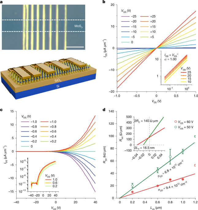
In response to the increasing needs of artificial intelligence computations and rising requirements in data centres and mobile devices, the necessity to fabricate transistors that are high-density, high-performance and energy-efficient has become increasingly urgent. For decades, the scaling of silicon has adhered to Moore’s law, yet it now approaches a challenging phase as it nears the physical limits of Si. Among the option for post-Si channel materials, two-dimensional (2D) materials emerge as the cornerstone for the continuing scaling of transistors 2 , offering potential advantages in low-power consumption. This miniaturization primarily depends on the scaling of channels and contacts, which involves not only shortening the channel length but also scaling down the size of metal contacts, the crucial gateways for current injection. This presents a marked challenge because shrinking their size can often lead to performance-limiting contact resistance. Substantial efforts have been made in understanding the scaling limitation for ultrathin 2D materials, in particular, on the channel scaling of monolayer (ML) 2D materials for the transistors beyond 1 nm technology node 3 , 4 . However, the equally important metal contact scaling has received very little attention, and it presents a tough challenge, especially for 2D material-based field-effect transistors (FETs), because their current crowding is expected to be prominent at the nanoscale contacts. …
Original source: Nature News